
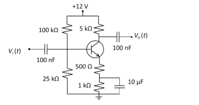
A small signal source, is applied to a BJT circuit. Assume zero source resistance, , , Early voltage and Thermal voltage . Which expression is the best approximation of the output voltage ?
Correct Answer :
Solution :
The correct answer is:
Step-by-Step Explanation:
1. DC Bias Analysis
From the given circuit diagram, we have the following component values:
Supply voltage: VCC = 12 V
Base divider resistors: R1 = 100 kΩ and R2 = 25 kΩ
Collector resistor: RC = 5 kΩ
Emitter resistors: RE1 = 500 Ω and RE2 = 1 kΩ
Transistor parameters: βdc = 99, VBE = 0.7 V, and Thermal voltage VT = 25 mV.
First, we find the Thévenin equivalent voltage (Vth) and resistance (Rth) at the base of the transistor:
Next, we write the Kirchhoff's Voltage Law (KVL) around the base-emitter loop:
Since :
Thus, the DC collector current is:
2. Small-Signal Parameter Calculations
Using the DC bias collector current, we compute the transconductance (gm) and the output resistance (ro) due to the Early effect:
3. Small-Signal Voltage Gain
For AC operation, the input and output coupling capacitors (100 nF) and the emitter bypass capacitor CE (10 μF) act as short circuits at the operating signal frequencies (ω = 105 rad/s and 107 rad/s).
Considering the configuration where the emitter is fully AC bypassed to maximize gain, the voltage gain (Av) of the common-emitter stage is given by:
Substituting the values:
4. Output Voltage Expression
The output voltage is the input signal scaled by the AC voltage gain:
Access expert-curated educational resources and study materials—completely free.
Create, conduct, and manage professional online assessments with Mindyard. Perfect for teachers and institutes.
Copyright © 2026 Mindyard. All Rights Reserved.