
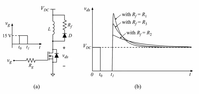
Consider the circuit shown in Figure (a). A gate pulse vg is applied between time instants t0 and t1. After t1, during the MOSFET turn OFF process, it experi ences a voltage overshoot. Based on the vds waveforms shown in Figure (b), which one of the following options is correct?
Correct Answer :
R3 ¿ R2 ¿ R1
Solution :
The correct option is R3 > R2 > R1 (represented in the options as R3 ¿ R2 ¿ R1).
Step-by-Step Explanation and Derivation:
1. Circuit Analysis during Switch Turn-OFF:
Consider the circuit shown in Figure (a). When the gate pulse vg is applied between time instants t0 and t1, the MOSFET is in the ON state, and current flows through the inductor L, storing magnetic energy. At t = t1, the gate voltage drops to 0 V, initiating the turn-off process of the MOSFET.
Because the current through the inductor L cannot change instantaneously, the stored energy forces the inductor current to freewheel. The freewheeling path consists of the diode D and the resistor Rf connected in series, and this combined branch is in parallel with the inductor L.
2. Expression for the Drain-to-Source Voltage:
The voltage across the MOSFET vds after turn-off is determined by the voltage at the drain node with respect to ground. Since the top of the inductor is connected to the DC source VDC, we can write:
Here, vL is the voltage across the inductor. Because the freewheeling branch is in parallel with the inductor, when the diode D is conducting, we have:
Assuming an ideal diode with negligible forward voltage drop (vD ≈ 0):
3. Relating Damping and Overshoot to Resistor Values:
During the transition, the parasitic drain-to-source capacitance of the MOSFET Cds interacts with the inductor L and the resistor Rf, forming a parallel resonant RLC network during the turn-off transient. The damping factor α of this parallel RLC network is given by:
This damping factor formula shows that the damping factor α is inversely proportional to the resistance Rf. Therefore:
- A larger resistance Rf corresponds to a smaller damping factor (underdamped response), resulting in a larger peak voltage overshoot and ringing.
- A smaller resistance Rf corresponds to a larger damping factor (closer to critically damped/overdamped response), resulting in a lower peak voltage overshoot.
From the waveforms in Figure (b), we observe the peak voltage overshoots for different values of Rf:
- The waveform with Rf = R1 has the highest overshoot (least damping).
- The waveform with Rf = R3 has an intermediate overshoot.
- The waveform with Rf = R2 has the lowest overshoot (most damping).
Thus, by comparing the peak values and the damping levels, we establish the following relation for the resistances:
- R1 (least damping/highest spike) is the smallest damping resistance.
- R2 (most damping/lowest spike) is the largest damping resistance.
Therefore, we conclude that:
Access expert-curated educational resources and study materials—completely free.
Create, conduct, and manage professional online assessments with Mindyard. Perfect for teachers and institutes.
Copyright © 2026 Mindyard. All Rights Reserved.