
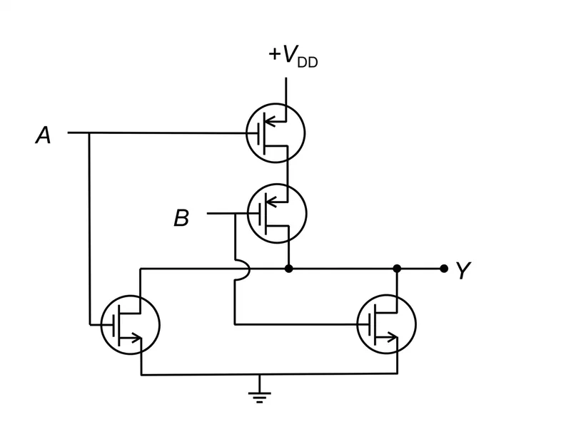
In the circuit shown in the Figure, A and B are logic inputs and Y is the logic output. Which of the following logic operations is realized by the circuit?
Correct Answer :
NOR
Solution :
The correct option is NOR.
By analyzing the provided circuit diagram, we can identify that it represents a classic Complementary Metal-Oxide-Semiconductor (CMOS) logic gate with inputs labeled A and B, a power supply voltage labeled +VDD at the top, a ground connection at the bottom, and an output terminal labeled Y. The circuit consists of two networks: a pull-up network (PUN) at the top and a pull-down network (PDN) at the bottom.
1. Pull-up Network (PUN):
The upper part of the circuit contains two PMOS transistors (indicated by the inward-pointing arrows on the gates) connected in series between the supply line +VDD and the output Y. The gates of these PMOS transistors are controlled by inputs A and B respectively.
- A PMOS transistor is active (ON) when its gate input is LOW (logic 0).
- Since the two PMOS transistors are connected in series, both must be ON simultaneously to create a conducting path from +VDD to the output Y.
- Therefore, the pull-up network only pulls the output Y to a HIGH state (logic 1) when:
and
2. Pull-down Network (PDN):
The lower part of the circuit consists of two NMOS transistors (indicated by the lack of bubbles or inward arrows at the gates) connected in parallel between the output Y and the ground.
- An NMOS transistor is active (ON) when its gate input is HIGH (logic 1).
- Since these two transistors are in parallel, the output Y will be connected to ground (logic 0) if either NMOS transistor or both are turned ON.
- Therefore, the pull-down network pulls the output Y to a LOW state (logic 0) if:
or (or both)
3. Truth Table Analysis:
Let us evaluate the output Y for all possible logic combinations of the inputs A and B:
• When A = 0 and B = 0: Both PMOS transistors are ON, and both NMOS transistors are OFF. The output Y is pulled up to +VDD (logic 1).
• When A = 0 and B = 1: The PMOS controlled by B is OFF, breaking the pull-up path. The NMOS controlled by B is ON, pulling Y to ground (logic 0).
• When A = 1 and B = 0: The PMOS controlled by A is OFF, breaking the pull-up path. The NMOS controlled by A is ON, pulling Y to ground (logic 0).
• When A = 1 and B = 1: Both PMOS transistors are OFF, and both NMOS transistors are ON. The output Y is pulled to ground (logic 0).
This behavior corresponds exactly to the truth table of a 2-input NOR gate. The logic expression for the output is:
Thus, the logic operation realized by the circuit is indeed NOR.
Access expert-curated educational resources and study materials—completely free.
Create, conduct, and manage professional online assessments with Mindyard. Perfect for teachers and institutes.
Copyright © 2026 Mindyard. All Rights Reserved.