
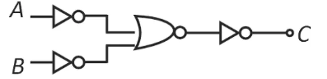
Which logic gate is given in the figure?
Correct Answer :
NAND
Solution :
To identify the logic gate represented by the given circuit diagram, we can analyze the output step-by-step from the inputs to the output:
1. Input NOT Gates:
Both inputs and are first passed through individual NOT gates.
The outputs of these NOT gates are:
- For input :
- For input :
2. NOR Gate:
The signals and are then fed into a NOR gate. The output of a NOR gate is the negation of the sum (OR) of its inputs:
3. Applying De Morgan's Law:
According to De Morgan's Law, the complement of the sum of two variables is equal to the product of their complements:
Substituting and into this law:
4. Final NOT Gate:
The output of the NOR gate, which is (equivalent to an AND gate configuration), is finally passed through a NOT gate to produce output :
The expression represents a NAND gate.
Access expert-curated educational resources and study materials—completely free.
Create, conduct, and manage professional online assessments with Mindyard. Perfect for teachers and institutes.
Copyright © 2026 Mindyard. All Rights Reserved.